确定
结果:搜索“
单面板
”相关内容
推荐
课程
文章
问答
文库
电子攻城狮之路
关注
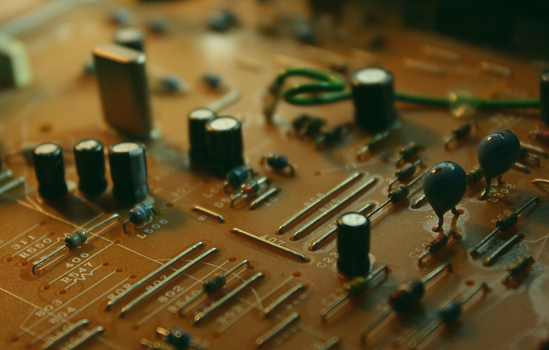
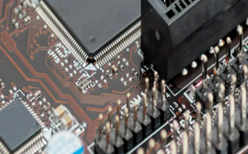
PCB单面焊盘设计:孔径设置要点
单面板因成本低、工艺简单,常用于低复杂度电路。但焊盘孔径设计不当易导致焊接不良或板子分层。以下从孔径设置原则出发,提炼关键设计要点。1、孔径设置核心原则基础公式孔径=引脚直径+0.2~0.5mm(预留公差,避免插不进或松动)。单面板需取上限
2026-01-15 11:19:45
文章
电子芯期天
本平台致力于分享各种电子电路开发设计资料及经验。
关注
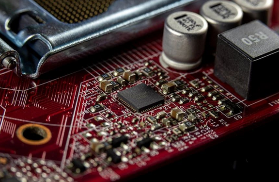
PCB单/双面板:3分钟看懂区别+避坑指南
电路板选单面还是双面?就像选单层公寓还是复式楼——单面板便宜简单,双面板灵活能装!但到底怎么选?直接看这篇,不绕弯子!1、单/双面板的核心区别结构差异单面板:只有一面有铜箔走线,元件焊在另一面(像“单面煎蛋”)。双面板:两面都有铜箔,用“过
2025-12-03 15:37:03
文章
电子攻城狮之路
关注
一表看懂FPC单/双面板在布局布线的不同
随着时代发展,柔性电路板(FPC)广泛应用,这也造成许多工程师会收到关于FPC板的项目设计,而FPC单面板与双面板在布局布线中存在显著差异,直接影响电路性能与制造成本,本文将从设计角度解析这两者的区别。1、结构差异单面板:仅一层导电铜箔,电
2025-07-11 15:35:41
文章
电子芯期天
本平台致力于分享各种电子电路开发设计资料及经验。
关注
不同层数的PCB板,如何选HDI阶?
HDI阶数直接影响PCB布线密度与制造成本,阶数越高,激光孔越复杂。本文从单面板到八层板,给出具体HDI阶数推荐,拒绝模糊建议。1、单面板(1层)场景:计算器、LED灯等简单设备。HDI阶数:❌ 不适用HDI:单层布线无需微孔技术。2、双面
2025-07-01 11:29:33
文章
电路之家
专注电子、科技分享,对电子领域深入剖解
关注
不同层数的PCB板,也要选用不同端接!
PCB层数直接影响信号完整性与制造难度,端接方式的选择需与层数精准匹配。本文从单面板到八层板,给出具体端接方案,拒绝泛泛而谈。1、单面板(1层)场景:计算器、LED灯等简单设备。端接方式:✅ 直接焊接:引脚与导线直接焊接,稳定性强。✅ 导线
2025-06-30 16:30:50
文章
电子攻城狮之路
关注
PCB单面板如何抄板,请注意这些细节!
PCB单面板作为电子设计中基础且常见的电路板类型,虽然简单但其技术性强要求精确,工程师通过遵循正确的抄板方法及注意事项,可确保抄板质量与原板一致,为后续的制作流程提供可靠的基础。1、PCB单面板的正确抄板方法①记录元件信息详细记录所有元件的
2025-02-18 09:25:50
文章
电子电路爱好者
关注
大学生毕业有必要再去PCB培训机构花钱学PCB设计
去年这个时候,我正抱着简历奔波于各大招聘会,却屡屡在PCB工程师岗位面试中碰壁。直到某次终面时,面试官指着我的课程设计作品说:"这种单面板布局和布线连电磁兼容测试都通不过,企业需要的是能做四层板以上、能满足各种EMC性能的的人才。"这句话让
2025-02-14 11:33:47
文章
吴川斌的博客
设计美学自媒体
关注
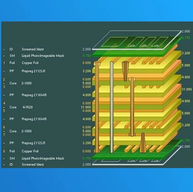
PCB多层板叠层设计之初体验
0 评论
2164 浏览
2024-10-14 15:00:15
文章
电路之家
专注电子、科技分享,对电子领域深入剖解
关注
PCB设计要连线交叉?如何高效做到!
在PCB设计中,我们总会遇到五花八门的设计要求,其中之一是连线交叉,如果在双面板或以上可以很容易实现,但在单面板设计中,由于布线空间的限制,连线交叉很难实现,因此,本文将直接列出几种针对连线交叉的具体解决方案,希望对小伙伴们有所帮助。1、跨
2024-09-19 10:10:28
文章
电子攻城狮之路
关注
FPC如何选择叠层结构?你该不会还在乱选吧?!
在快速发展的电子行业中,柔性电路板(FPC)靠着优越的柔韧性、轻薄及高可靠性等特点,是众多消费电子不可缺少的桥梁,而FPC的叠层结构设计,将直接关系着其性能表现和应用场景。那么FPC如何选择叠层结构?1、单面板单面板是最基础的FPC结构,采
2024-07-18 09:39:43
文章
凡亿助教-小燕
专注电子设计,好文分享
关注
PCB种类大全都在这了,小白速戳!
作为电子元器件的支撑和电气连接的提供者,印刷电路板(PCB)在电子行业中扮演着至关重要的角色,根据不同的分类标准,PCB可划分为多种类型,那么你知道有哪些PCB吗?它们有什么不同?1、结构分类单面板:最简单的PCB,仅在一面有铜箔,另一面是
2024-05-07 15:43:37
文章
凡亿教育
湖南凡亿智邦电子科技有限公司
关注
Cadence Allegro 23.1-Allegro X软件速成160讲
9443
8
视频
电子攻城狮之路
关注
单面板抄板技术解析:从拆卸到复制全过程
作为电子制造中的基础组件,单面板抄板过程虽然简单,但需要遵循一系列专业步骤,单面板的抄板过程有元器件记录、拆卸与清洗、图像获取、图像处理、软件转换、打印对比及测试等,本文将谈谈这些,希望对小伙伴们有所帮助。1、元器件记录与拍照首先,详细记录
2024-02-24 10:30:34
文章
电子攻城狮之路
关注
双面板抄板技术解析:从扫描到生产全过程
众所周知,印刷电路板(PCB)按照层数多少,可分为单面板、双面板及多层板。双面板作为电子制造中的关键组件,其抄板过程需要高度的专业性和精确度,下面来看看如何抄板。1、扫描线路板首先,使用高精度扫描仪对双面板的上下表层进行扫描,生成两张清晰的
2024-02-23 15:18:22
文章
嵌入式大杂烩
分享嵌入式电子级设计的经验、心得、程序设计架构及测试
关注
单面板/双面板/多层板的内层如何制作?
按照PCB板的层数不同,可分为单面板、双面板和多层板,虽然都属于PCB板,但制作流程却有很大的明显,身为电子工程师的你,知道它们是如何制作吗?今天凡小亿开课谈谈它们的制作工艺,希望对小伙伴们有所帮助。需要注意的是,相比多层板,单面板和双面板
2023-12-22 10:59:12
文章
电路之家
专注电子、科技分享,对电子领域深入剖解
关注
单面板、双面板及多层板的正确抄板方法
提起抄板,很多电子工程师不会陌生,抄板也叫做反向工程或逆向工程,是一种通过分析已有电子产品的电路板,并尝试复制或再创建其结构和功能的过程,抄板的方法因电路板的类型和技术参数而异,下面来看看有哪些?1、单面板的抄板单面板通常只有一面有导电路线
2023-10-17 15:49:41
文章
嵌入式大杂烩
分享嵌入式电子级设计的经验、心得、程序设计架构及测试
关注
如何根据产品需求选择单面板还是多层板?
随着时代高速发展,多层板逐渐成为市场上最火的PCB类型,颇有与单面板一较高下的气势,这也给很多电子工程师提出了难题,如何根据项目需求来合理选择,单面板还是多层板?顾名思义,单层板只有一层基材,也叫做基板,而多层板则有多层基材,它们的区别如下
2023-10-14 14:23:08
文章
凡亿助教-小燕
专注电子设计,好文分享
关注
为什么PCB多层板设计越来越受欢迎?
随着时代高速发展,越来越多电子工程师开始放弃PCB单面板设计,选择多层板设计,这是由于多种因素及市场所决定,那么我们来看看为什么PCB多层板设计越来越受欢迎?1. 高密度集成电路现代电子产品求更高的性能和更小的尺寸。高密度集成电路(IC)变
2023-09-05 11:24:16
文章
电子攻城狮之路
关注
Altium难题:如何在单面板顶层设置不覆盖绿油?
0 评论
7636 浏览
2023-09-01 15:25:51
文章
凡亿助教-小燕
专注电子设计,好文分享
关注
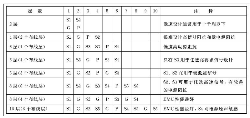
多层印制电路板(PCB)的电磁兼容性设计指南(上)
之前我们讨论了单面板或双面板的电磁兼容性设计,但若是在高速逻辑电路时,当这两个PCB无法满足电磁兼容性要求,我们应研究多层板的应用。今天我们来讨论下多层板应如何设计,才能满足电磁兼容性要求。一般来说,在进行多层PCB设计时,应先考虑带宽和等
2022-12-08 14:34:31
文章

 2026-01-15 11:19:45


 9443
9443
 8
8