凡亿教育-小燕
凡事用心,一起进步打开APP
公司名片全能19期-allegro_THE的_第三次作业[2]千兆网卡PCB设计

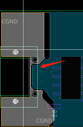
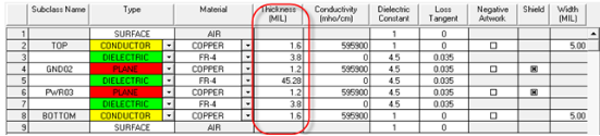
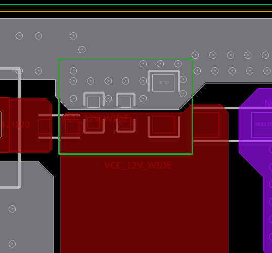
注意电源地跟机壳地之间满足至少2MM间距:
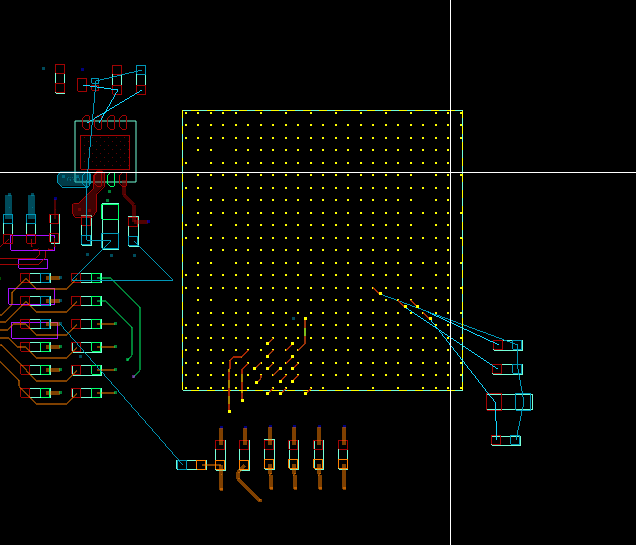
器件注意放置完全,并且放置完成之后走线连接:
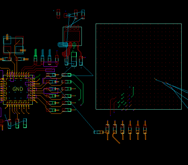
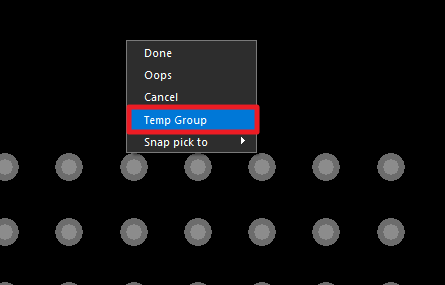
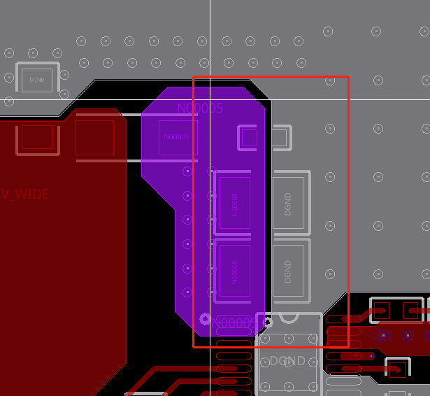
把没有设计的器件布局布线设计下。
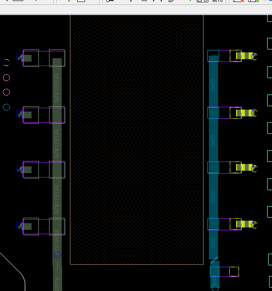
变压器除了差分信号,其他信号也要走线连接完全:
还存在多处飞线,存在信号没有连接完全:
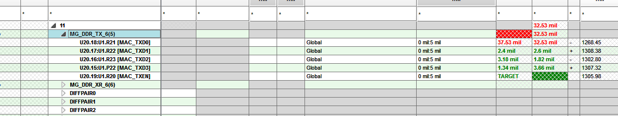
等长线之间需要满足3W间距:
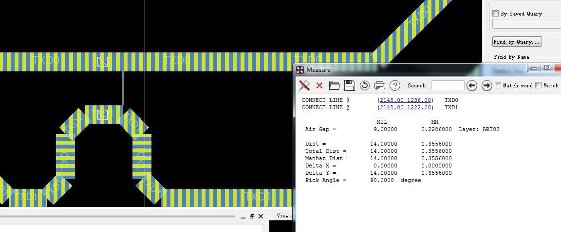
注意等长还存在误差报错:
声明:本文内容及配图由入驻作者撰写或者入驻合作网站授权转载。文章观点仅代表作者本人,不代表凡亿课堂立场。文章及其配图仅供工程师学习之用,如有内容图片侵权或者其他问题,请联系本站作侵删。
相关阅读
进入分区查看更多精彩内容>


暂无评论